
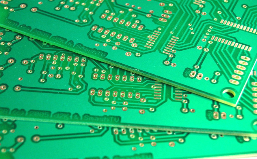
As electronic devices become more compact and functionally advanced, the demand for efficient circuit design has increased significantly. While single-sided and double-sided boards are suitable for simple applications, more complex systems require additional layers to improve performance and reduce size. One of the most commonly used solutions in modern electronics is the 4 layer PCB, which offers a balanced combination of performance, cost, and design flexibility.
Understanding how 4 layer PCBs are structured, manufactured, and used can help engineers and businesses choose the right solution for their electronic projects.
What Is a 4 Layer PCB?
A 4-layer PCB is a multilayer printed circuit board that consists of four conductive layers separated by insulating materials. These layers typically include two outer layers for component placement and routing, and two inner layers that are often used as power and ground planes.
This configuration allows for improved signal integrity, reduced electromagnetic interference, and more efficient routing compared to single-sided or double-sided boards.
4 layer PCBs are widely used in applications that require moderate complexity, high performance, and compact design.
Structure of a 4 Layer PCB
The structure of a 4 layer PCB is carefully designed to optimize electrical performance and reliability. The board typically consists of four copper layers arranged in a stack-up with insulating layers between them.
The top layer is used for component placement and signal routing. Below it is an inner layer that often serves as a ground plane, providing a stable reference for signals.
The third layer is usually a power plane, distributing power evenly across the board. The bottom layer is used for additional signal routing and component connections.
The insulating layers, commonly made from materials such as FR4, separate the copper layers and provide electrical insulation.
Vias are used to connect the layers, allowing signals and power to travel between different parts of the board.
Manufacturing Process of 4 Layer PCBs
The manufacturing of a 4 layer PCB involves multiple steps to ensure precision and reliability. The process begins with preparing the inner layers by laminating copper onto the substrate and etching the desired circuit patterns.
Once the inner layers are ready, they are stacked with insulating prepreg layers and outer copper foils. The stack is then bonded together through a lamination process under heat and pressure.
Drilling is performed to create vias and holes for component mounting. These holes are plated with copper to establish electrical connections between layers.
The outer layers are then patterned using photolithography and etching to form the final circuit design.
A solder mask is applied to protect the copper traces, followed by the silkscreen layer for labeling.
Finally, the board undergoes testing and inspection to ensure it meets quality and performance standards.
Advantages of 4 Layer PCBs
One of the main advantages of a 4 layer PCB is improved signal integrity. The use of dedicated power and ground planes helps reduce noise and ensures stable signal transmission.
Another benefit is reduced electromagnetic interference. The internal layers act as shielding, minimizing interference between signals.
4 layer PCBs also allow for higher component density. With additional layers available for routing, designers can create more compact and efficient layouts.
Thermal management is improved as well, as the internal planes help distribute heat across the board.
Additionally, these boards provide a good balance between performance and cost. While more expensive than double-sided boards, they are still more affordable than higher-layer PCBs.
Applications of 4 Layer PCBs
The versatility of 4 layer PCB technology makes it suitable for a wide range of applications. In consumer electronics, these boards are used in devices such as smartphones, tablets, and laptops.
In the automotive industry, 4 layer PCBs are used in control systems, sensors, and infotainment systems.
Industrial equipment also relies on these boards for automation systems, control panels, and monitoring devices.
Telecommunications equipment, including routers and networking devices, uses 4 layer PCBs for efficient signal processing.
Medical devices such as diagnostic equipment and monitoring systems also benefit from the reliability and performance of 4 layer PCBs.
Their ability to support complex circuits while maintaining compact size makes them ideal for modern electronic designs.
Design Considerations for 4 Layer PCBs
Designing a 4 layer PCB requires careful planning to ensure optimal performance. Engineers must consider the stack-up configuration, including the arrangement of signal, power, and ground layers.
Proper impedance control is essential for maintaining signal integrity, especially in high-speed designs.
Component placement should be optimized to minimize signal path lengths and reduce interference.
Via design is also important. The placement and size of vias can affect both electrical performance and manufacturing complexity.
Thermal management should be considered, particularly for high-power applications. Proper design can help dissipate heat and maintain stable operation.
Manufacturing constraints must also be taken into account to ensure the design can be produced efficiently.
Limitations of 4 Layer PCBs
While 4 layer PCBs offer many advantages, they also have some limitations. One of the main drawbacks is higher cost compared to single-sided and double-sided boards.
The manufacturing process is more complex, requiring additional steps and precise alignment of layers.
Design complexity is also higher, requiring experienced engineers to optimize performance.
However, these limitations are often outweighed by the benefits of improved performance and compact design.
Conclusion
The 4 layer PCB is a versatile and efficient solution for modern electronic applications that require improved performance, reduced interference, and compact design. Its multilayer structure enables better signal integrity, higher component density, and enhanced reliability.
As electronic devices continue to evolve, 4 layer PCBs will remain a popular choice across industries such as consumer electronics, automotive, industrial, and telecommunications. Businesses seeking high-quality and reliable circuit boards often collaborate with an experienced 4-layer PCB manufacturer to ensure precision, consistency, and optimal performance in their electronic products.
